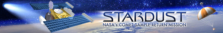
|
Stardust was launched carrying two microchips
approximately the size of a thumbnail. Two copies
of each chip were installed on the spacecraft
(for a total of four chips). Two of the microchips
(#1 & #2) are inside the Sample Return Capsule,
and will return back to Earth with the capsule
in the year 2006. Due to public demand and interest
a second set of microchip where installed on the
spacecraft body and will remain in space forever.
Note that these microchips are not electronic
parts like a computer chip, but are actually a
silicon wafers. The names are placed onto the
wafer chip through a technique called Electron
Beam Lithography.The wafer is 4 inches square
initially and comes with a layer of silicon oxide
on its surface.. The wafer is coated with a thin
photographic film of photo-resist PMMA (pexiglass).
The names are stored on a VAX computer and converted
into a format usable by the electron beam lithography
tool. The data is read and fed into the electron
beam tool which engraves the names into the PMMA
surface of the wafer chip using a highly-focused
electron beam. The names can be written multiple
times to the wafer if we want to make multiple
copies of the small microchip. The wafer then
goes through a process similar to developing film,
where the wafer is rinsed in a developer that
removes exposed PMMA (or the area written on by
the electron beam). The next step is to coat the
wafer with a thin metal film (titanium & platinum).
This is done by placing it in a vacuum chamber
and heating a small amount of the metal, which
evaporates and coats the wafer by condensing on
it. The wafer chip is then placed in a solvent
which dissolves away the remaining PPMA and any
metal attached to it, leaving behind the letters
of the names. Finally, the wafer is cut up into
1x1 centimeter-sized square chips.

| Last updated
November 26, 2003 |
|